
Hong Kong
CNN
—
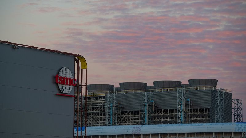
TSMC says its second manufacturing facility in Arizona will probably be delayed, marking one other setback for the world’s largest chipmaker and its function in US President Joe Biden’s bid to spice up American manufacturing.
The power will now be operational in 2027 or 2028, in comparison with previous expectations of a 2026 begin, in line with Chairman Mark Liu.
“There will probably be a spot,” he informed analysts on an earnings name Thursday.
Liu stated development on the shell of the manufacturing facility had begun, however the Taiwanese chipmaking titan wanted to overview “how a lot incentives … the US authorities can present.”
The corporate is in shut contact with US officers on the matter, together with dialogue of tax credit, he added.
It’s the second time TSMC (TSM), the world’s largest chipmaker, has been compelled to push again its plans within the western US state.
It introduced in 2022 that it might construct a second semiconductor plant in Arizona, including to plans for an present fab and elevating its overall investment within the state from $12 billion to $40 billion. A fab refers to a semiconductor fabrication plant.
The funding has beforehand been lauded by Biden as an indication that US manufacturing “is again.”
However final yr, the corporate stated manufacturing at its first fab would be delayed from 2024 to 2025, as a result of a scarcity of specialist staff.
The corporate may be rethinking which kind of merchandise will probably be made. Initially, TSMC had announced the primary facility would produce 4-nanometer chips, and the second would make 3-nanometer chips, that are among the many most superior semiconductors.
However on Thursday, Liu steered that plans for its second fab had been in flux, saying the scale of presidency incentives would decide the sort of expertise deployed.
The primary facility continues to be on observe for manufacturing of 4-nanometer expertise, which can begin within the first half of 2025, stated the manager.
TSMC, based mostly within the Taiwanese metropolis of Hsinchu, produces an estimated 90% of the world’s super-advanced semiconductors and provides to world tech giants reminiscent of Apple (AAPL) and Nvidia (NVDA).
It mass produces parts which can be very important to the operating of all the things from smartphones to washing machines.
The corporate has sometimes saved its most superior manufacturing at residence in Taiwan, however it has been increasing overseas in recent times as a result of business strain and encouragement from various governments. Final yr, it announced a manufacturing facility in Dresden, Germany, its first in Europe.
The producer has been constructing a facility in Japan, which can formally open subsequent month, Liu stated Thursday. Mass manufacturing on the plant, situated within the prefecture of Kumamoto, stays on schedule for the fourth quarter of 2024, he added.
TSMC can also be contemplating whether or not to open a second facility in Japan.
“The second fab in Japan is in severe analysis stage,” and the agency is holding talks with the federal government, in line with Liu.
Liu informed analysts the abroad expansions had been in response to “at the moment’s fractured globalization setting.”
On Thursday, TSMC stated it had weathered a difficult yr in 2023 because of the weakening world financial system, which weighed on demand.
However “our enterprise has bottomed out,” CEO C.C. Wei stated on the decision.
The corporate shared a a lot brighter outlook for the yr forward, projecting a 20% leap in 2024 income.
It cited a boon for the worldwide semiconductor trade from “the rising emergence of generative AI-related purposes,” which embrace widespread platforms reminiscent of ChatGPT.
TSMC’s shares climbed 9.8% in New York on Thursday following its earnings report, and rose by 6.5% on Friday in Taipei.